Introduction
In broad terms, the task of power electronics is to process and control the flow of electric energy by supplying voltages and currents in a form that is optimally suited for user loads.
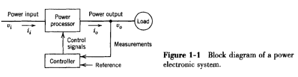
Figure 1-1 shows a power electronic system in a block diagram form. The power input to this power processor is usually (but not always) from the electric utility at a line frequency of 60 or 50 Hz, single phase or three phases. The phase angle between the input voltage and the current depends on the topology and the control of the power processor. The processed output (voltage, current, frequency, and the number of phases) is as desired by the load. If the power processor’s output can be regarded as a voltage source, the output current and the phase angle relationship between the output voltage and the current depend on the load characteristic. Normally, a feedback controller compares the output of the power processor unit with a desired (or a reference) value, and the error between the two is minimized by the controller. The power flow through such systems may be reversible, thus interchanging the roles of the input and the output.
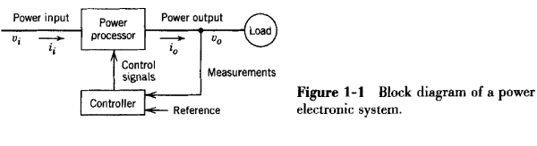
In recent years, the field of power electronics has experienced a large growth due to confluence of several factors. The controller in the block diagram of Fig. 1-1 consists of linear integrated circuits and/or digital signal processors. Revolutionary advances in microelectronics methods have led to the development of such controllers. Moreover, these advances in semiconductor fabrication technology have made it possible to significantly improve the voltage- and current-handling capabilities and the switching speeds of power semiconductor devices, which make up the power processor unit of Fig. 1-1. At the same time, the market for power electronics has significantly expanded. Electric utilities in the United States expect that by the year 2000 over 50% of the electrical load may be supplied through power electronic systems such as in Fig. 1-1.
Power Electronics Defined
It has been said that people do not use electricity, but rather they use communication, light, mechanical work, entertainment, and all the tangible benefits of both energy and electronics. In this sense, electrical engineering is a discipline very much involved in energy conversion and information. In the general world of electronics engineering, the circuits engineers design and use are intended to convert information, with energy merely a secondary consideration in most cases. In radio frequency applications, energy and information are sometimes on a more equal footing, but the main function of any circuit is that of information transfer.
What about the conversion and control of electrical energy itself? Electrical energy sources are varied and of many types. It is natural, then, to consider how electronic circuits and systems can be applied to the challenges of energy conversion and management. This is the framework of power electronics, a discipline that is defined in terms of electrical energy conversion, applications, and electronic devices. More specifically,
DEFINITION: Power electronics involves the study of electronic circuits intended to control the flow of electrical energy. These circuits handle power flow at levels much higher than the individual device ratings.
Power Electronics Vs Linear Electronics
In any power conversion process such as that shown by the block diagram in Fig. 1- 1, a small power loss and hence a high energy efficiency is important because of two reasons: the cost of the wasted energy and the difficulty in removing the heat generated due to dissipated energy.
Other important considerations are reduction in size, weight, and cost. The above objectives in most systems cannot be met by linear electronics where the semiconductor devices are operated in their linear (active) region and a line-frequency transformer is used for electrical isolation. As an example, consider the direct current (dc) power supply of Fig. 1-2a to provide a regulated output voltage V, to a load.
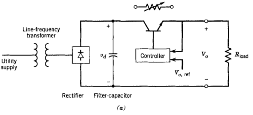

The utility input may be typically at 120 or 240 V and the output voltage may be, for example, 5 V. The output is required to be electrically isolated from the utility input. In the linear power supply, a line-frequency transformer is used to provide electrical isolation and for stepping down the line voltage. The rectifier converts the alternating current (ac) output of the transformer low-voltage winding into dc. The filter capacitor reduces the ripple in the dc voltage vd. Figure 1-2b shows the vd waveform, which depends on the utility voltage magnitude (normally in a t 10% range around its nominal value).
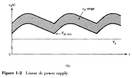
The transformer turns ratio must be chosen such that the minimum of the input voltage v, is greater than the desired output V. For the range of the input voltage waveforms shown in Fig. 1-2b, the transistor is controlled to absorb the voltage difference between v and V, thus providing a regulated output. The transistor operates in its active region as an adjustable resistor, resulting in a low energy efficiency. The line-frequency transformer is relatively large and heavy.
In power electronics, the above voltage regulation and the electrical isolation are achieved, for example, by means of a circuit shown in Fig. 1-3a.
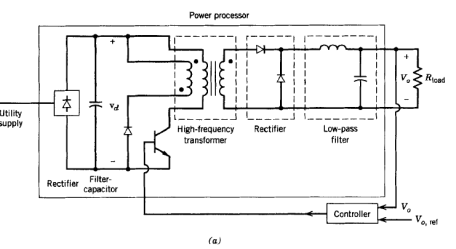

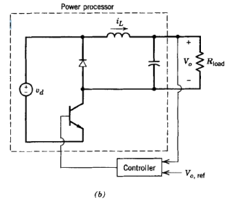
In this system, the utility input is rectified into a dc voltage vd, without a line-frequency transformer. By operating the transistor as a switch (in a switch mode, either fully on or fully 0ff) at some high switching frequency f, for example at 300 kHz, the dc voltage vd is converted into an ac voltage at the switching frequency. This allows a high-frequency transformer to be used for stepping down the voltage and for providing the electrical isolation.
In order to simplify this circuit for analysis, we will begin with the dc voltage vd as the dc input and omit the transformer, resulting in an equivalent circuit shown in Fig. 1-3b.

Suffice it to say at this stage that the transistor diode combination can be represented by a hypothetical two-position switch shown in Fig. 1-4a (provided iL(t) > 0).
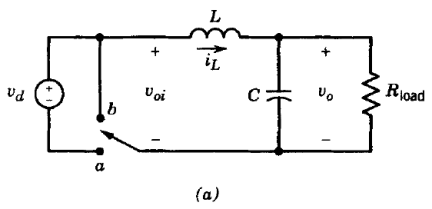
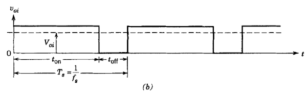
The switch is in position a during the interval t-on, when the transistor is on and in position b when the transistor is off during t-off. As a consequence, Voi equals Vd, and zero during t-on and t-off, respectively, as shown in Fig. 1-4b.
Let us define
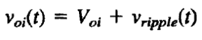
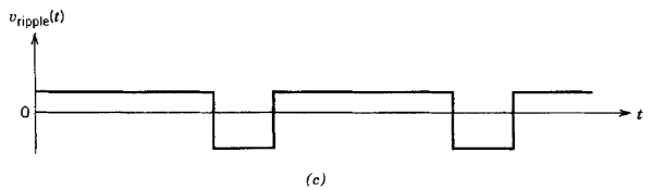
where Voi is the average (dc) value of Voi-t, and the instantaneous ripple voltage V-ripple, which has a zero average value, is shown in Fig. 1-4c.
The L-C elements form a low-pass filter that reduces the ripple in the output voltage and passes the average of the input voltage, so that
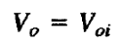
where Vo, is the average output voltage. From the repetitive waveforms in Fig. 1-4b, it is easy to see that
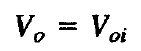

As the input voltage Vd changes with time, Eq. 1-3 shows that it is possible to regulate Vo, at its desired value by controlling the ratio t-on/Ts which is called the duty ratio D of the transistor switch. Usually, Ts (= l/fs) is kept constant and t-on is adjusted.
There are several characteristics worth noting. Since the transistor operates as a switch, fully on or fully off, the power loss is minimized. Of course, there is an energy loss each time the transistor switches from one state to the other state through its active region. Therefore, the power loss due to switchings is linearly proportional to the switching frequency. This switching power loss is usually much lower than the power loss in linear regulated power supplies.
At high switching frequencies, the transformer and the filter components are very small in weight and size compared with line-frequency components.
Scope and Applications of Power Electronics
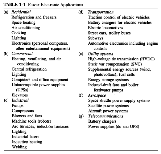
The expanded market demand for power electronics has been due to several factors discussed below:
- Switch-mode (dc) power supplies and uninterruptible power supplies. Advances in microelectronics fabrication technology have led to the development of computers, communication equipment, and consumer electronics, all of which require regulated dc power supplies and often uninterruptible power supplies.
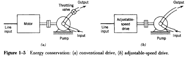
- Energy conservation. Increasing energy costs and the concern for the environment have combined to make energy conservation a priority. One such application of power electronics is in operating fluorescent lamps at high frequencies (e.g., above 20 kHz) for higher efficiency. Another opportunity for large energy conservation is in motor-driven pump and compressor systems. In a conventional pump system shown in Fig. 1-5a, the pump operates at essentially a constant speed, and the pump flow rate is controlled by adjusting the position of the throttling valve. This procedure results in significant power loss across the valve at reduced flow rates where the power drawn from the utility remains essentially the same as at the full flow rate. This power loss is eliminated in the system of Fig. 1-56, where an adjustable-speed motor drive adjusts the pump speed to a level appropriate to deliver the desired flow rate.
- Process control and factory automation. There is a growing demand for the enhanced performance offered by adjustable-speed-driven pumps and compressors in process control. Robots in automated factories are powered by electric servo (adjustable-speed and position) drives. It should be noted that the availability of process computers is a significant factor in making process control and factory automation feasible.
- Transportation. In many countries, electric trains have been in widespread use for a long time. Now, there is also a possibility of using electric vehicles in large metropolitan areas to reduce smog and pollution. Electric vehicles would also require battery chargers that utilize power electronics.
- Electro-technical applications. These include equipment for welding, electroplating, and induction heating.
- Utility-related applications. One such application is in transmission of power over high-voltage dc (HVDC) lines. At the sending end of the transmission line, line-frequency voltages and currents are converted into dc. This dc is converted back into the line-frequency ac at the receiving end of the line. Power electronics is also beginning to play a significant role as electric utilities attempt to utilize the existing transmission network to a higher capacity. Potentially, a large application is in the interconnection of photovoltaic and wind-electric systems to the utility grid.
Classification of Power Processors and Converters
For a systematic study of power electronics, it is useful to categorize the power processors, shown in the block diagram of Fig. 1-1, in terms of their input and output form or frequency.
In most power electronic systems, the input is from the electric utility source. Depending on the application, the output to the load may have any of the following forms:
- dc
- regulated (constant) magnitude
- adjustable magnitude
- ac
- constant frequency, adjustable magnitude
- adjustable frequency and adjustable magnitude
The utility and the ac load, independent of each other, may be single phase or three phase. The power flow is generally from the utility input to the output load.
The power processors of Fig. 1-1 usually consist of more than one power conversion stage (as shown in Fig. 1-6) where the operation of these stages is decoupled on an instantaneous basis by means of energy storage elements such as capacitors and inductors.
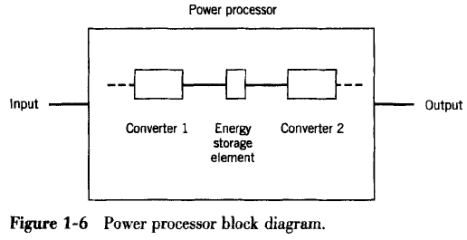
Therefore, the instantaneous power input does not have to equal the instantaneous power output. We will refer to each power conversion stage as a converter. Thus, a converter is a basic module (building block) of power electronic systems. It utilizes power semiconductor devices controlled by signal electronics (integrated circuits) and possibly energy storage elements such as inductors and capacitors. Based on the form (frequency) on the two sides, converters can be divided into the following broad categories:
- ac to dc
- dc to ac
- dc to dc
- ac to ac
We will use converter as a generic term to refer to a single power conversion stage that may perform any of the functions listed above. To be more specific, in ac-to-dc and dc-to-ac conversion, rectifier refers to a converter when the average power flow is from the ac to the dc side. Inverter refers to the converter when the average power flow is from the dc to the ac side.
Further insight can be gained by classifying converters according to how the devices within the converter are switched. There are three possibilities:
- Line frequency (naturally cornmutated) converters, where the utility line voltages present at one side of the converter facilitate the turn-off of the power semiconductor devices. Similarly, the devices are turned on, phase locked to the line voltage waveform. Therefore, the devices switch on and off at the line frequency of 50 or 60 Hz.
- Switching (forced-commutated) converters, where the controllable switches in the converter are turned on and off at frequencies that are high compared to the line frequency.
- Resonant and quasi-resonant converters, where the controllable switches turn on and/or turn off at zero voltage and/or zero current.
Interdisciplinary Nature of Power Electronics
The discussion in this introductory chapter shows that the study of power electronics encompasses many fields within electrical engineering, as illustrated by Fig. 1- 10.
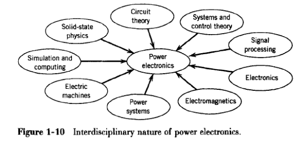
Combining the knowledge of these diverse fields makes the study of power electronics challenging as well as interesting. There are many potential advances in all these fields that will improve the prospects for applying power electronics to new applications.
Sources:
- Power Electronic – Mohan
- Libro Rashid – Power Electronic Handbook
Literature Review by: Larry Francis Obando – Technical Specialist
Lunes 15 de noviembre, 11:08 am – Caracas, Quito, Guayaquil.
Escuela de Ingeniería Eléctrica de la Universidad Central de Venezuela, Caracas.
Escuela de Ingeniería Electrónica de la Universidad Simón Bolívar, Valle de Sartenejas.
Escuela de Turismo de la Universidad Simón Bolívar, Núcleo Litoral.
Contact: Ecuador (Quito, Guayaquil, Cuenca) telf. +34633129287
WhatsApp: +34633129287
email: dademuchconnection@gmail.com