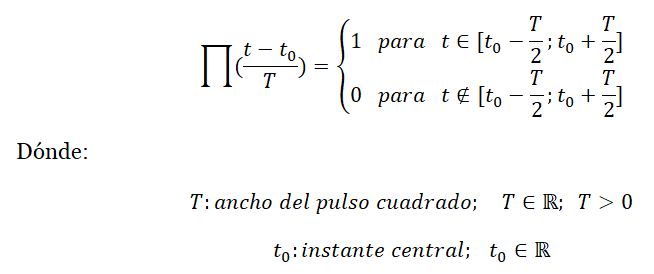
La señal pulso cuadrado es aquella señal analógica cuya amplitud es 1 para un cierto intervalo finito de valores de la variable independiente y 0 en el resto:
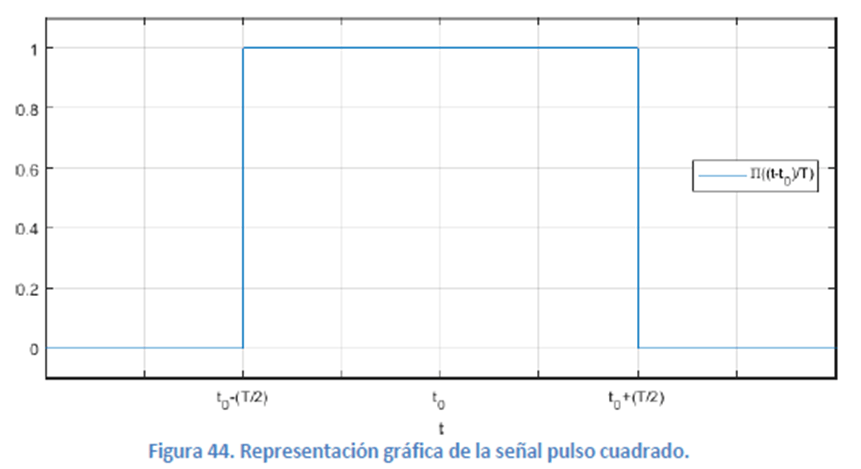
La forma gráfica del puso cuadrado es:
Se observa que la señal pulso cuadrado permite acotar fácilmente cualquier señal finita analógica definida entre t1 y t2, simplemente definiendo T y t0 de modo tal que t1=t0-T/2 y t1=t0+T/2. Sin embargo, para definir de forma compacta tanto una señal analógica definida por intervalos como el período básico de una señal periódica analógica, sigue siendo más útil la señal escalón unitario analógica. La razón de esto está en que los intervalos de definición de la señal escalón unitario normalmente son cerrados por la izquierda y abiertos por la derecha, mientras que el intervalo de definición de la señal pulso cuadrado es cerrado por ambos lados. Es justamente por esta razón por la cual la señal pulso cuadrado no puede ser expresada como la diferencia de dos escalones unitarios analógicos: el límite por la izquierda está incluido en el intervalo de definición de la señal pulso cuadrado. Es también por esta razón que tiene sentido definir la señal pulso cuadrado en el dominio analógico, pero no en el dominio digital. Si quisiéramos definir una versión digital de la señal pulso cuadrado, no tendríamos más que restar dos escalones unitarios digitales desplazados.
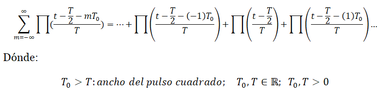
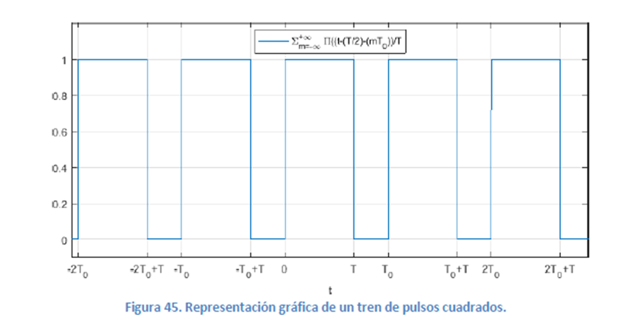
Una señal periódica muy interesante puede definirse a partir de la señal pulso cuadrado: el tren de pulsos cuadrados de ancho T y período fundamental T0:
La representación gráfica del tren de pulsos cuadrados se muestra a continuación:
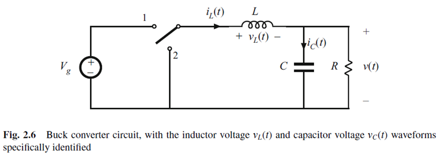
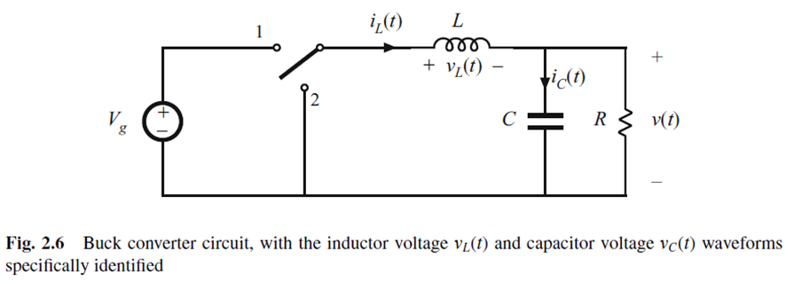
Let us more closely examine the inductor and capacitor waveforms in the buck converter illustrated in Figure 2-6.
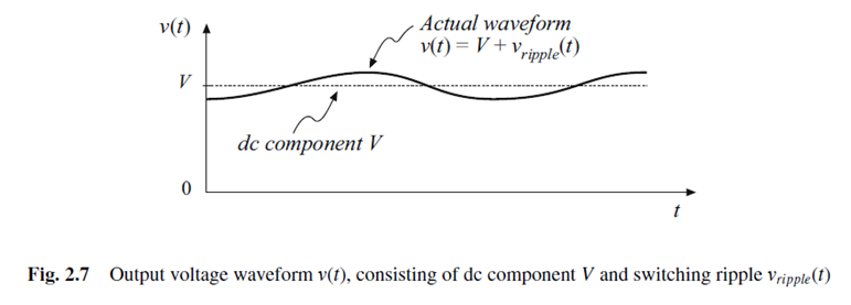
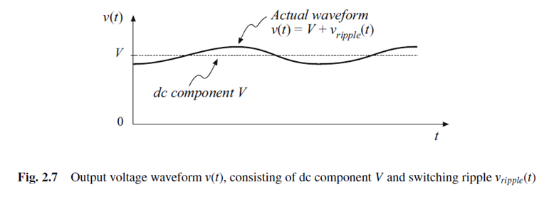
Actually, the output voltage appears as illustrated in Figure 2-7.
This approximation is known as The small ripple approximation or the linear ripple approximation.
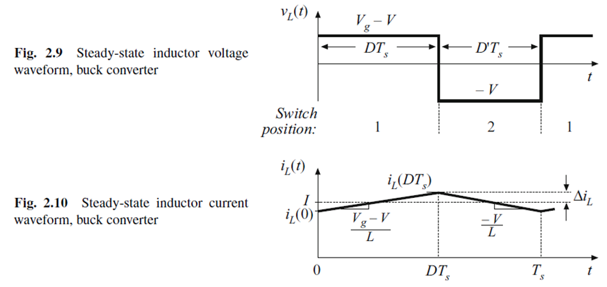
With this approximation, let us analyze the inductor current waveform. Since the inductor voltage is essentially constant during the first interval (switch in position 1), the inductor current slope of equation (6) is also essentially constant and the inductor current increase linearly, as in Figure 2-10:
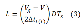
Solution for L yields:
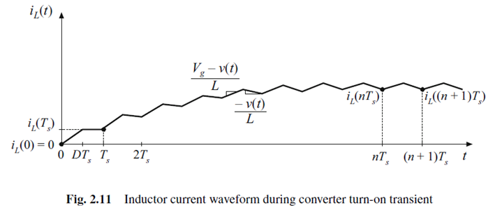
Equations (1) to (3) and Figure 2.10 are derived under steady-state conditions. Let us consider next what happens to the inductor current when the converter is first turned on. Suppose that the inductor current and output voltage are initially zero, and an input voltage Vg is the applied. As shown in Figure 2.11, during the first subinterval, with the switch position in 1, we know that the inductor current will increase.
Since the inductor current iL(t) flows to the output, the output capacitor will charge slightly, and will v(t) increase slightly too. The process repeats during the second and succeeding switching periods, with inductor current iL(t) increasing during each subinterval 1 and decreasing during each subinterval 2.
As the output capacitor continues to charge and v(t) increases, the slope during each subinterval 1 decreases and the slope during each subinterval 2 becomes more negative. There is no change in the inductor current over a complete switching period and the converter reachs the steady state condition.
The requirement that, in equilibrium, the net change in inductor current over one switching period be zero lead us to a way to find steady-state condition in any switching converter. That is what we call the inductor volt-second balance.
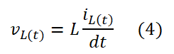
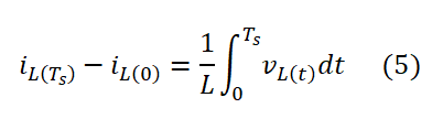
Given the defining relation of an inductor:
Integration over one complete switching period, say from t=0 to t=Ts yields:
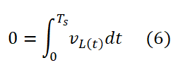
In steady-state condition, the initial and final value of the inductor current is equal, so:
The right hand of equation (6) has the units of volt-second or flux-linkages. It states that the total area, or net volt-seconds, under the vL(t) waveform must be zero under steady-state condition.
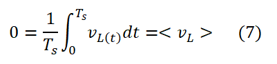
An equivalent form is obtained by dividing both sides of equation (6) by the switching period:
Equation (7) is recognized as the average value, or DC component, of vL(t). Equation (7) states that, under steady-state condition, the applied inductor voltage must have zero DC component.
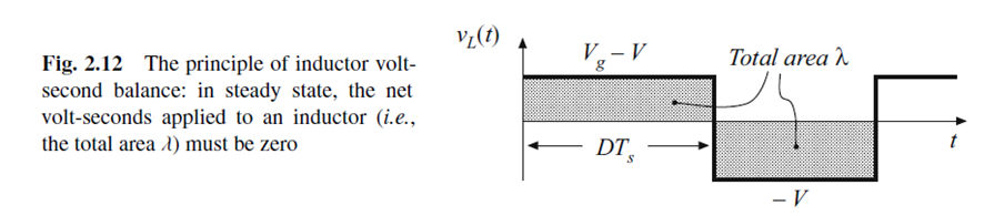
The inductor voltage waveform is reproduced in Figure 2.12 with the area, or net volt-seconds, under the vL(t) curve identified.
The total area lambda is given by the areas of the two rectangles:
The average value is therefore:
What lead us to state, using equation (2), that:
Considering Figure 2.3, the output voltage v(t) of a Buck Converter is essentially equal to the DC component of the switching voltage vs(t), and equation (10) states that the output voltage v(t) is less than or equal to the input voltage Vg, since 0<D<1.
Source:
Erickson R., Maksimovic D. Fundamentals of Power Electronics. Pp. 22-24.
Examinemos más de cerca las formas de onda del inductor y el capacitor en el convertidor reductor ilustrado en la figura 2-6.
En la práctica, es imposible construir un filtro de paso bajo perfecto que elimine por completo los componentes de CA en las frecuencias de conmutación y sus armónicos. Por lo tanto, el filtro de paso bajo debe permitir que al menos una pequeña cantidad de los armónicos de alta frecuencia generados por el interruptor alcancen el voltaje de salida. En realidad, el voltaje de salida aparece como se ilustra en la Figura 2-7.
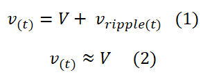
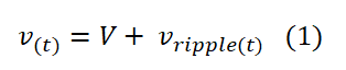
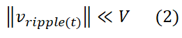
Por lo tanto, el voltaje de salida real v(t) consta del componente de CC deseado V, más un pequeño componente de CA no deseado vripple(t) que surge de la atenuación incompleta de los armónicos de conmutación por el filtro de paso bajo. Sin embargo, la magnitud de vripple(t) se ha exagerado en la figura 2-7. Casi siempre es una buena aproximación suponer que la magnitud de vripple(t) es mucho menor que el componente de CC, V:
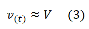
Por lo tanto, el voltaje de salida v(t) está bien aproximado por su componente de CC, V:
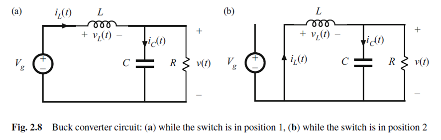
Esta aproximación se conoce como Small ripple approximation (aproximación de ondulación pequeña) o la aproximación de ondulación lineal. Con esta aproximación, reemplazamos las expresiones sinusoidales amortiguadas o exponenciales para las formas de onda del inductor y el capacitor con formas de onda lineales más simples. Esta aproximación está justificada siempre que el período de conmutación sea más corto que las constantes de tiempo naturales del circuito. Además, esta aproximación debe aplicarse solo a variables continuas: la corriente del inductor y el voltaje del capacitor. No cambiar el voltaje, cambiar la corriente del voltaje del inductor. A continuación, analicemos la forma de onda de la corriente del inductor. Con el interruptor en la posición 1, el circuito se reduce a la figura 2.8a.
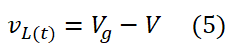
La tensión del inductor vL(t) viene dada por:
Aplicando la aproximación de pequeña ondulación a la ecuación (3):
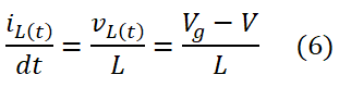
La corriente del inductor se puede encontrar mediante el uso de la definición:
Dado que el voltaje del inductor es esencialmente constante durante el primer intervalo (interruptor en la posición 1), la pendiente de corriente del inductor de la ecuación (6) también es esencialmente constante y la corriente del inductor aumenta linealmente, como en la Figura 2-10, donde podemos ver vL(t) frente a iL(t):
Se aplican argumentos similares en el segundo intervalo (interruptor en la posición 2). El lado izquierdo del inductor está conectado a tierra, lo que conduce al circuito de la figura 2.8b.
El uso de la aproximación de ondulación pequeña conduce a:
así:
En consecuencia, durante el segundo intervalo, la corriente del inductor disminuye linealmente en una ecuación de pendiente constante (8), como en la figura 2-10, posición 2 del interruptor.
En la figura 2-10, la corriente del inductor iL(t) es simétrica con respecto a I. Dado que:
es el pico de ondulación (peak ripple), el pico a pico de ondulación (peak to peak ripple) es:
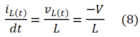
El pico a pico es también el cambio en la corriente, es igual a la pendiente por la longitud del primer intervalo DTs:
Solución para el pico a pico de ondulación conduce a:
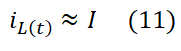
Los valores típicos de la ondulación máxima se encuentran en el rango del 10 % al 20 % del valor a plena carga del componente I de CC. Por lo tanto, por diseño, la ondulación de corriente del inductor también suele ser pequeña en comparación con el componente I de CC. se justifica la aproximación:
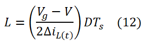
La solución para L en la ecuación (10) produce:
La ecuación (12) se usa comúnmente para seleccionar el valor de la inductancia en el diseño del convertidor reductor. Es importante recalcar que las ecuaciones (1) a (12) se derivan de condiciones de estado estacionario.
Fuente:
Erickson R., Maksimovic D. Fundamentals of Power Electronics. Pp18-22.
Let us more closely examine the inductor and capacitor waveforms in the buck converter illustrated in Figure 2-6.
In practice, it is impossible to build a perfect low-pass filter that completely removes the AC components at the switching frequencies and its harmonics. So, the low-pass filter must allow at least some small amount of the high-frequencies harmonics generated by the switch to reach the output voltage. Actually, the output voltage appears as illustrated in Figure 2-7.
So, the actual output voltage v(t) consists of the desired DC component V, plus a small undesired AC component vripple(t) arising from the incomplete attenuation of the switching harmonics by the low-pass filter. However, the magnitude of vripple(t) has been exaggerated in Figure 2-7. It is nearly always a good approximation to assume that the magnitude of vripple(t) is much smaller than the DC component V:
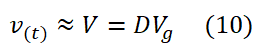
Therefore, output voltage v(t) is well approximated by is DC component V:
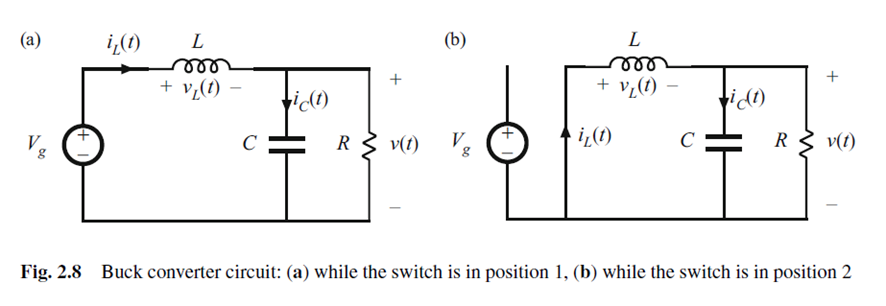
This approximation is known as The small ripple approximation or the linear ripple approximation. With this approximation, we replace the exponential or damped sinusoidal expressions for the inductor and capacitor waveforms with simpler linear waveforms. This approximation is justified provided that the switching period is shorter than the natural time constants of the circuit. Also, this approximation must be applied just to continuous variables: the inductor current and the capacitor voltage. Not to switching voltage, switching current of inductor voltage. Next, let us analyze the inductor current waveform. With the switch in position 1, the circuit reduces to Figure 2.8a.
The inductor voltage vL(t) is given by:
Applying small ripple approximation to equation (3):
The inductor current can be found by use of the definition:
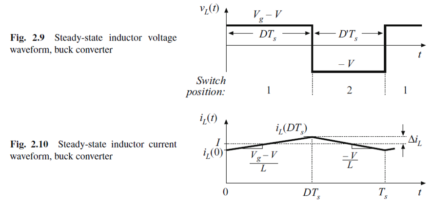
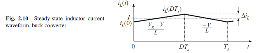
Since the inductor voltage is essentially constant during the first interval (switch in position 1), the inductor current slope of equation (6) is also essentially constant and the inductor current increase linearly, as in Figure 2-10, where we can see vL(t) vs iL(t):
Similar arguments apply in the second interval (switch in position 2). The left side of the inductor is connected to ground, leading to the circuit of Figure 2.8b.
Using the small-ripple approximation leads to:
So:
Consequently, during the second interval the inductor current decrease linearly at a constant slope equation (8), as in Figure 2-10 position 2 of the switch.
In Figure 2-10 the inductor current iL(t) is symmetrical about I. Since:
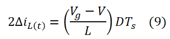
is the peak ripple, the peak to peak ripple is:
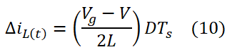
Which is also the change in current . It is equal to the slope times the length of the first interval DTs:
Solution for the peak ripple yields:
Typical values of the peak ripple lie in the range of 10%-20% of the full-load value of the DC componentI. So, by design, the inductor current ripple is also usually small compared to the DC component I. The small approximation is justified:
Solution for L in equation (10) yields:
Equation (12) is commonly used to select the value of the inductance at the design of the buck converter. Equations (1) to (12) are derived from steady-state conditions. Source:
Erickson R., Maksimovic D. Fundamentals of Power Electronics. Pp18-22.
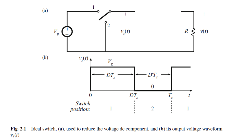
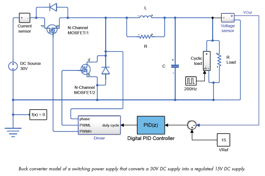
The buck converter has been built to reduce the DC voltage, using only nondissipative switches, inductor and capacitors. The switch produces rectangular waveform vs(t) as illustrated in Figure 2-1.
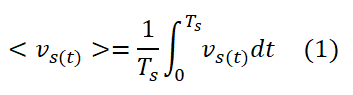
In practice, the switch is realized using power semiconductor devices, such as transistors and diodes, which are controlled to turn off and on as required to perform the function of the ideal switch. The switching frequency fs is in the range of 1KHz – 1MHz, depending on the switching speed of the semiconductor devices. The duty ratio D is the fraction of time that the switch spends in position 1, and is a number between zero and one. The complement of the duty ratio, D’, is defined as (1- D). As we know from Fourier Transform, the DC component of a periodic function as vs(t), is given by its average value <vs(t)>:
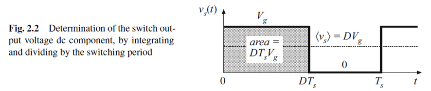
Solving equation (1) we obtain the following solution as illustrated in Figure 2-2:
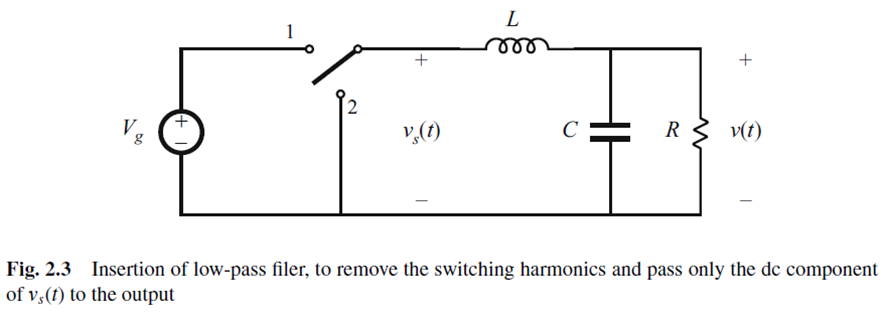
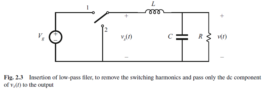
Equation (2) confirms that the DC component of the voltage output vs(t) of the buck converter is equal to or lower than the input voltage vg. In the practice, vs(t) is not ideal, so it has harmonic components. In consequence, the converter has to have a filter integrated on it. What remains is to insert a low-pass filter as illustrated in Figure 2-3:
The filter is designed to pass the DC component of vs(t), but to reject its components at the switching frequency and its harmonics. To accomplish this, we design the filter such that its cutoff frequency is much lower than the switching frequency. So, the output v(t) voltage from Figure 2-3, is essentially equal to the DC component of vs(t):
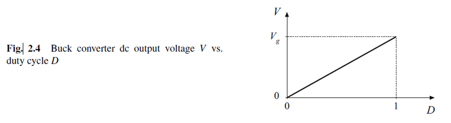
The network of Figure 2-3 allows control of the output. Figure 2-4 is the control characteristic of the buck converter:
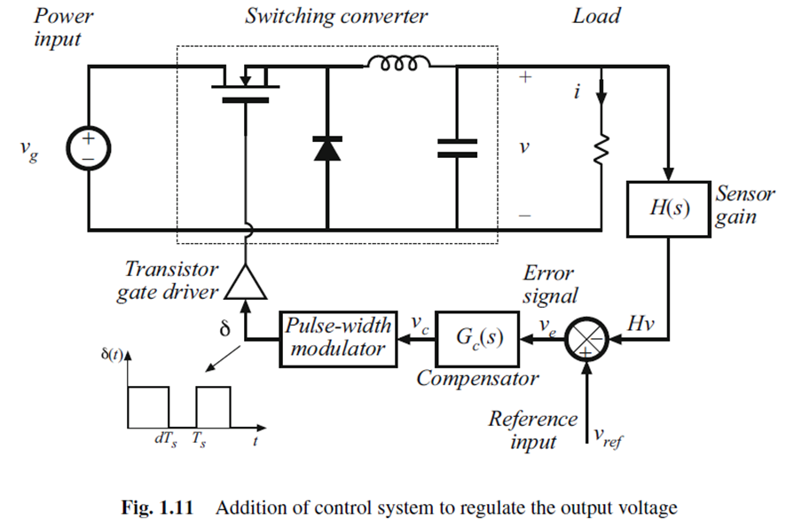
So, the buck converter has a linear control characteristic. Feedback systems are often constructed that adjust the duty ratio D to regulate the converter output voltage, such as in Figure 1.11:
Simulation with Matlab-Simulink
Source:
Erickson R., Maksimovic D. Fundamentals of Power Electronics.Pp15-18.
La linéarité est l’une des propriétés les plus importantes des systèmes. Ce cours en ligne se compose de trois vidéos à partir desquelles vous apprendrez à analyser la propriété de linéarité et à vérifier qu’un système est linéaire ou non. Il vous propose une théorie et des méthodes équivalentes aux cours Signaux et Systèmes en Ingénierie. La propriété de linéarité est vérifiée pas à pas dans ces 5 systèmes à temps continu et/ou discret présentés ci-dessous:
Linearität ist eine der wichtigsten Eigenschaften von Systemen. Dieser Online-Kurs besteht aus drei Videos, in denen Sie lernen, die Linearitätseigenschaft zu analysieren und zu überprüfen, ob ein System linear ist oder nicht. Es bietet Ihnen Theorie und Methoden, die den Signals and Systems-Klassen in den Ingenieurwissenschaften entsprechen. Die Eigenschaft der Linearität wird Schritt für Schritt in diesen 5 unten gezeigten kontinuierlichen und/oder diskreten Zeitsystemen verifiziert:
Linearity is one of the most important properties of systems.
Linearity is one of the most important properties of systems. This Online course consists of three videos from which you will learn to analyze the linearity property and check that a system is Linear, or otherwise, that it is not. It offers you theory and methods that are equivalent to the Signals and Systems classes in Engineering. The property of linearity is verified step by step in these 5 continuous and/or discrete time systems shown below:
La Linealidad es una de las propiedades más importantes de los sistemas.
La Linealidad es una de las propiedades más importantes de los sistemas. Este curso Online consta de tres videos de los que aprenderás a analizar la propiedad de linealidad y demostrar que un sistema es Lineal, o en caso contrario, que no lo es. Te ofrece teoría y métodos que son equivalentes al de las clases de Señales y Sistemas en Ingeniería. Se analizan los 5 sistemas de tiempo continuo y/o discreto que se muestran a continuación: